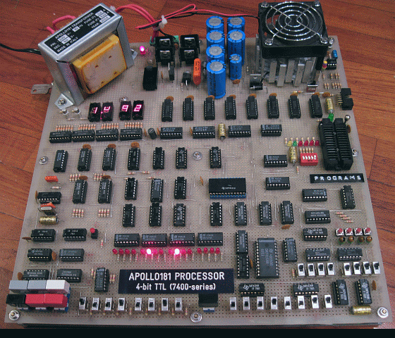
A homemade board using TTL to emulate a 4-bit processor from the 1970's. This setup uses approximately 600 gates. In today's Intel 22 nm die, over 100,000,000 transistors fit onto the head of a ball-point pen, but this technology is nearing its max potential.
[Image Source: http://ygg-it.tripod.com/]
Since the introduction of current-generation Silicon-based transistors, it has been known that limits exists to the technology. This is evident within the article “The non-volatile memory challenge” circa 1997, where Electro-Physicist Mark Dax reports the issues ahead concerning the advancement of transistor switching and its inevitable wall, preventing it from progressing along previous trends. Dax states, “The ability to dimensionally scale without affecting output signal is a desirable characteristic for memory devices, since it means that device redesign effort is reduced when feature sizes decrease.” This demonstrates the need for a device capable of such scalability, which is a feature current Silicon-based transistors do not own. Dax presents sets of equations that prove the plateau of the Silicon based transistor’s scalability while also suggesting alternative solutions, one of the solutions being ferroelectric gating.
As mentioned, researchers saw this issue arrive in the math nearly two decades before the proper tooling existed and it was physically proven. Correlated Oxide switches do not have these limitations imposed on them. The term “Correlated Oxides” is referred to by Taka-hisa Arima of the Research for Advanced Materials team at Tohoku University in Japan as an “observation of sliding charge-density waves [of electrons]” (“Correlated Oxides: Sliding electrons take charge”, 12). The method of ferroelectric gating takes advantages of the “wave”-like characteristics of these Correlated Oxides, which are known to be unique to them alone. In comparison to traditional gating which uses a small input current to transition an insulator to a conductor, ferroelectric gating uses a “small electric field that initiates a collective motion of a large number of otherwise immobilized electrons” (“Correlated Oxides: Sliding electrons take charge”, 13) .
Today’s processors consist of a matrix of transistors, spaced a distance apart so as to prevent the electromagnetic field of its neighbor from interacting upon each other. With the introduction of correlated oxide switching and the byproduct of the smaller electromagnetic field, this distance can shrink, allowing for smaller packages, in addition to its quicker nature. This benefit serves a major roles to meeting the demands of Moore’s Law, that is, that memory capacity will double each two years due to enhanced manufacturing techniques, improving upon a template architecture.
Evidence for the necessity of a new transistor technology is also evident in the Harvard study conducted by Martin Dominik. Upon shrinking below the 20 nm mark, the experiment outlined in the article “Downscaling ferroelectric field effect transistors by using ferroelectric Si-doped [Hafnium],” Martin proved that the EMF gives enough current to the gate that it inadvertently switches states, referred to by the industry as a nuisance trip. In this experiment, the equations mentioned by Dax were physically demonstrated, as the “package threshold” was found to be 16 nm, while current transistors in consumer processor operate at 22 nm. The previous generation of processor was 26 nm to demonstrate how close the consumer market is to the architecture’s plateau and the technology fails to meet demands of Moore’s Law.
